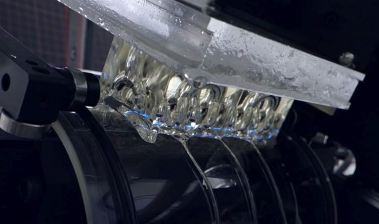
A close-up photograph of the RECILS three-dimensional printer in action.© The University of Tokyo
People are increasingly turning to 5G, or fifth-generation, devices to take advantage of features such as gigabyte-per-second download speeds. Although 5G networks are still being rolled out, telecommunication engineers are already seeking higher frequency bandwidths that will be able to accommodate massive future growth in data traffic. Now, a new additive manufacturing approach called RECILS can help researchers rapidly produce prototypes of complex parts for telecommunication systems with a resolution comparable to the width of a human hair.
Cylinders put a twist on resin printing
Stereolithography three-dimensional (3D) printing uses laser light to harden liquid resins into solid plastics. Unlike the more familiar extrusion-style 3D printers, stereolithography printers chemically bond all the layers together into lightweight structures that have high mechanical strength. And because the printer’s lateral resolution is determined mainly by the micrometre-scale diameter of the laser beam, this technology can produce objects with exceptionally fine detail for applications ranging from product design to customized dental implants.
Surprisingly, the biggest obstacle facing stereolithography comes from a fundamental design flaw. “In conventional stereolithography, we have to remove the object from a flat glass window when we’re done printing,” explains Junji Yumoto, an emeritus professor at the University of Tokyo and a laser physics expert. “This base layer can become quite wide, and we have to pull it out with a lot of force,” he says. “All of that force can concentrate onto narrow points in the 3D-printed object, causing it to break.”

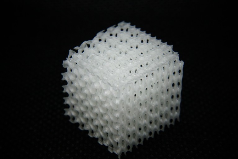
A mesh structure fabricated using RECILS.© The University of Tokyo
In 2014, Yumoto and his colleagues, including engineers on loan from Sony, overcame this problem by adopting a novel approach. They created a one-dimensional gap by positioning a glass cylinder as a base window a few tens of micrometres from a planar building platform (PBP). A nozzle feeds precise amounts of resin into the gap as the ultraviolet laser beam scans along the one-dimensional gap. The PBP moves perpendicular to the laser scanning direction in synch with the laser scan. While each line is cured, the PBP rolls off the cylinder, automatically detaching the build before the next line is created. This synchronized motion of the laser scan and the PBP forms a two-dimensional plate below the building platform through a line-by-line operation. “This concept makes fabrication times 33–50% faster than those of conventional stereolithography because we no longer need the peeling process,” says Yumoto.
During initial tests, the team took videos of their new printer in action. After one such session, one of Yumoto’s colleagues had an epiphany. “When we played the moulding process backwards, the operation looked the same as that of a hand-held slicer used to slice ham or cheese. So we coined the name RECILS — slicer in reverse.”
Hitting the sweet spot for microchannels
Yumoto notes that most 3D printers currently target two types of applications: larger objects tens to hundreds of centimetres in size or tiny materials no bigger than a few millimetres. “There’s a giant gap in the market for palm-sized objects with a resolution between 20 and 30 micrometres,” he says.

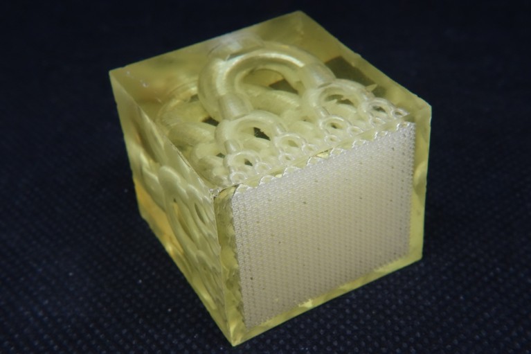
A structure printed using RECILS in which one inlet channel splits into 2,048 outlets.© The University of Tokyo
One lightly explored area is microchannel devices for lab-on-a-chip applications in chemistry and medicine. Microfluidic chips are currently produced by lithographic etching and stamping of silicone polymers — processes that are difficult to scale up for commercial ventures. While 3D printing offers the ability to rapidly produce intricate channel structures, the resolution of the channel widths can be several times lower than typical printed features.
The unique features of the RECILS printer, however, make printing 3D microchannels as simple as pushing a button. “In our system, the one-dimensional gap works with the laser beam spot to provide fine control of the hollow shapes,” says Yumoto. “And since we don’t need the peeling process, we can fabricate very complex 3D structures. For example, in one case, a single inlet channel divided into 2,048 outlets.”
3D printed waveguides
Microchannels are also predicted to play a role in the future of optical communications because bandwidths beyond 5G need to be accessed using waveguides — hollow tubes than can propagate electromagnetic radiation with little power loss. “If you look at some of the standards for making microwave waveguides, they need precise shapes on the order of a few hundred micrometres,” says Yumoto. “This can be really difficult to achieve using conventional machining.”

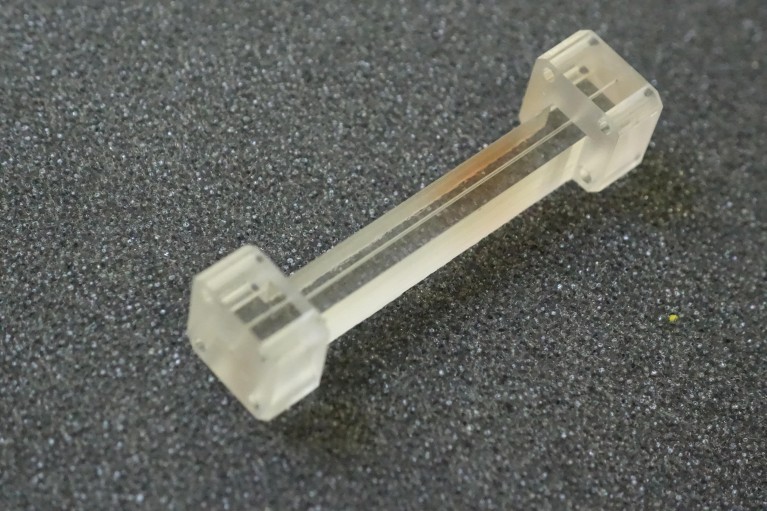
A waveguide structure produced using RECILS.© The University of Tokyo
Experiments with RECILS indicate that the printer can make short work of manufacturing waveguides, producing high-precision prototypes. After plating the resin structures with a metal coating, the researchers were able to steer terahertz microwave signals whose frequencies are 1,000 times higher than today’s cellular network bands.
“The manufacturing of waveguides is quicker and cheaper than other equipment, and it provides a freedom in structure and design of devices,” says Yumoto. “If we made the same objects with a metal 3D printer, the surface roughness wouldn’t be nearly as good.”
Rooting for the little guy
RECILS is now focusing on providing printing services to manufacturers through PhotonTech Innovations, a venture company established to commercialize research from the University of Tokyo. “It’s usually difficult for professors or students to tap into bigger markets, but it’s critical — such a small business can encourage and stimulate other fields in unexpected ways,” concludes Yumoto.


