Thank you for visiting nature.com. You are using a browser version with limited support for CSS. To obtain
the best experience, we recommend you use a more up to date browser (or turn off compatibility mode in
Internet Explorer). In the meantime, to ensure continued support, we are displaying the site without styles
and JavaScript.
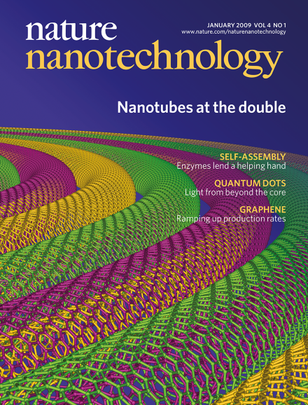
Double-walled carbon nanotubes are ideal systems for studying the interwall interactions that influence the properties of nanotubes with two or more walls. However, current synthesis techniques produce unwanted single- and multi-walled nanotubes. Alexander Green and Mark Hersam have now shown that density-gradient ultracentrifugation can be used to separate doublewalled nanotubes from mixtures of single- and multi-walled nanotubes. The cover image is a schematic representation showing the atomic structure of an array of double-walled nanotubes; the diameter of each nanotube is approximately 2 nm.
The commercial success of low-tech nano-enabled products, such as sports equipment and lubricants, could pave the way for more advanced nanodevices and applications.
The commercial success of products based on giant magnetoresistance is often cited as a reason for supporting basic physics research. The reality is more complex, given the range of bodies, including IBM and the US military, involved in developing new technologies based on this Nobel-prize-winning discovery.
The differences between the sciences and the humanities have been debated in academic circles for decades. Chris Toumey explores how nanotechnology fits into this picture and how the nature of science itself is a legitimate subject for researchers in the humanities and social sciences.
Protein nanoparticles derived from viruses are commonly studied, but a new rod-shaped thermophilic virus isolated from acidic hot springs may yield another class of protein building blocks that are stable and can be selectively modified with diverse chemical groups.
Two independent groups have demonstrated an unprecedented degree of control over the crystal structure and defect distribution in semiconductor nanowires
The production of functional molecular architectures through self-assembly is commonplace in nature, but it is still a major challenge to achieve similar complexity in the laboratory. It has now been shown that reversible enzyme-catalysed reactions can drive synthetic self-assembly. This approach could ultimately lead to the fabrication of functional nanostructures with enhanced complexities and fewer defects.
Graphene is a promising material for the next-generation of nanoelectronic devices, but it has been difficult to produce single-layer samples in bulk quantities. A solution-based process for the large-scale production of single-layer, chemically converted graphene has now been demonstrated and used to make field-effect devices with currents that are three orders of magnitude higher than previously reported for chemically produced graphene.
Most techniques for producing graphene use graphite as a starting material and are labour-intensive. The direct chemical synthesis of carbon nanosheets in gram-scale quantities from the common laboratory reagents ethanol and sodium has now been demonstrated. The ability to produce bulk graphene samples from non-graphitic precursors with a scalable, low-cost approach should take us a step closer to real-world applications of graphene.
Nanogenerators based on piezoelectric nanowires have already been demonstrated, but these devices were not mechanically robust. A new approach overcomes such problems by avoiding sliding contacts. Repeatedly stretching and releasing a piezoelectric wire in the new devices can generate electricity with an efficiency of 6.8%.
Previous photodetectors based on solution-processed colloidal quantum dots have demonstrated either rapid response times or high sensitivity. Researchers have now taken advantage of new insights into charge transport in these devices to build photodiodes that offer both rapid response times and high sensitivity.
The mechanical deposition of single molecules on a surface can be optically monitored with nanometre precision using a combination of total internal reflection fluorescence microscopy and atomic force microscopy.
The growth temperature and diameter of indium arsenide nanowires have been tuned to fabricate highly–reproducible polytypic and twin–plane superlattices within single nanowires. In addition to reducing defect densities, this level of control should also lead to band–gap engineering and novel electronic behaviour.
Current methods for synthesizing double-wall carbon nanotubes also produce single- and multi-wall nanotube impurities. Density gradient ultracentrifugation has now been used to separate double-wall nanotubes from such mixtures. The resulting material has distinct advantages over single-wall nanotubes when used in transparent conductors.