The annual global market for laser equipment is estimated at $60 billion – with industries from manufacturing, medicine and measurement to sensing, lighting, and entertainment, all reliant on it.
High-power lasers cut, drill, solder, etch and weld most of today’s electronics and metal components, for example, notes Eiji Yagyu, the chief researcher at Mitsubishi Electric, in Tokyo, Japan. Of these processes cutting demands the most power – usually a beam of more than 1 kW.
“Laser diodes, and solid, or fibre, lasers are the main technologies used in manufacturing today, accounting for 60–70% of the market,” says Yagyu. But low energy-consuming lasers, such as laser diodes, will become increasingly important to carbon conscious economies, he says.
Laser diodes are directly driven by an electric current, he explains, while solid and fibre lasers have less efficient power conversion. However, the take-up of laser diodes has lagged behind fibre lasers in manufacturing, because they struggle to reach the same beam quality and focus at high outputs.

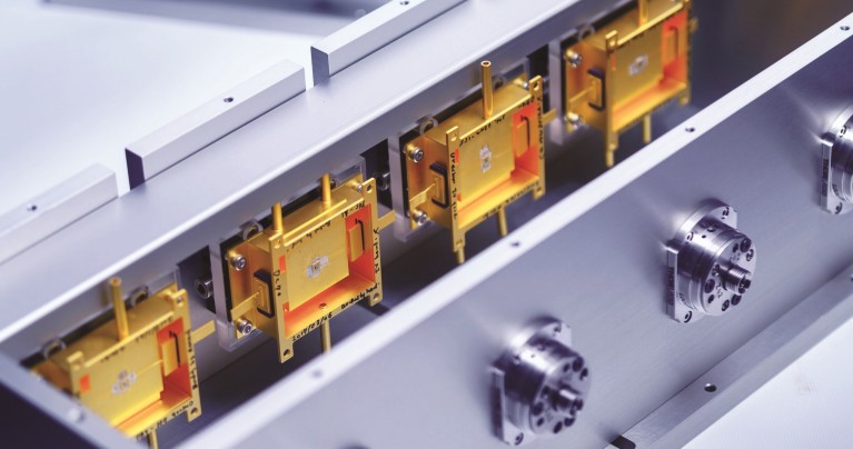
An array of PCSELs from 2017 has recently been surpassed by one with five lasers.
FOCUSED POWER
With laser diodes, the larger the surface of the active material producing the laser light, known as a resonator, the greater the output power. But increasing the area of the resonator also distorts the laser beam, reducing beam quality, explains Kazuki Kuba, a deputy manager at Mitsubishi Electric’s Advanced Technology R&D Centre.
To address this challenge, Yagyu and Kuba’s team are working with Kyoto University on developing new photonic-crystal surface-emitting lasers (PCSELs), a type of laser diode. These contain a photonic crystal structure (the resonator) and an active layer, sandwiched between doped semiconductor cladding layers, with metal electrodes on the top and bottom. Laser light photons are created by the semiconductors and photonic crystal in response to the direct input of an electrical current.
Unlike other laser diodes that use a pair of mirrors to create one-dimensional resonance, PCSELs utilize two-dimensional resonance created by numerous partial reflections and diffractions in the photonic crystal. This allows PCSELs to achieve both high beam quality and high output power over large areas, says Kuba.
Currently, continuous-wave powers as high as 20–25 watts can be reached with conventional single laser diodes, but the beam quality is extremely poor. PCSELs, however, can reach powers in the tens of watts while preserving beam quality, and Mitsubishi Electric is striving to achieve PCSELs capable of 100 watts within the next few years.
PCSEL MODULE
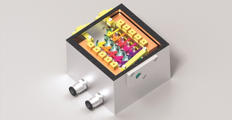
In collaboration with Kyoto University, Mitsubishi Electric have already designed a PCSEL module that integrates ten individual PCSELs arranged in two arrays each comprising five PCSELs. Each array of five PCSEL beams is linked to a dichroic mirror, which causes near-infrared light to be split up into distinct beams of different wavelengths, which are then combined by another mirror, known as a polarization mirror. In this way, the laser beams from the ten PCSELs are combined into one very powerful and high-quality beam.

A 1-kW PCSEL for cutting small enough to fit in the palm of your hand may be ready by 2023, and is a fraction of the size of today’s fibre-laser equivalent.
This PCSEL system is also much more space efficient. A 1-kW module fits in the palm of your hand, while an equivalent fibre-laser system, currently in use at Mitsubishi Electric factories, is roughly 50 x 50 x 10 centimetres in size.
“We think that marking barcodes and symbols on products will be one the first industrial applications,” says Yagyu. “But as higher-power PCSEL modules are developed, we expect to see PCSEL-based laser processing systems used across a range of industrial manufacturing applications, including metal cutting.”
However, to achieve the necessary power for metal cutting, each of the ten PCSELs that make up the module need to have a power of 100 watts, which isn’t yet possible.

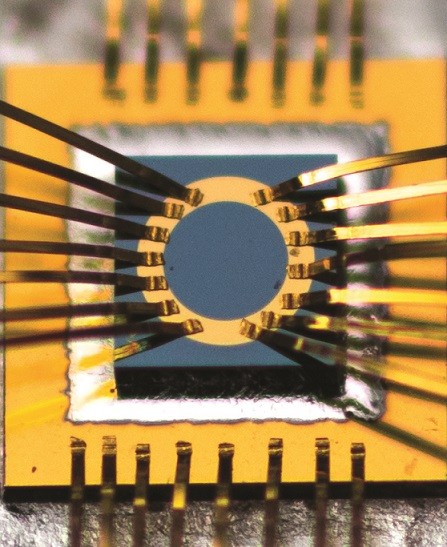
Tiny 500-micrometre-scale PCSELs developed at Kyoto University (bottom right) may reduce sizes further.
One group that works closely with Mitsubishi Electric, led by Susumu Noda from the Centre of Excellence (COE) for Photonic-Crystal Surface-Emitting Lasers at Kyoto University, is steadily moving towards these types of power levels. In 2021, they demonstrated a 2‑mm‑diameter PCSEL with an output power of 29 W.
Yagyu says that to scale up to 100 W of power, the PCSELs need to be 3–4 mm in diameter. “But increasing the size still distorts the laser beam too much.”
Noda says his group expects to achieve usable 100-W PCSELs within the year. Yagyu says that Mitsubishi Electric’s PCSELs, designed for eventual mass-production, may be available in prototype form as soon as next year.
“We expect to be producing 1 kW PCSEL modules soon afterwards,” he says. “And we anticipate that Mitsubishi Electric will be producing high-power PCSELs by 2026 and laser processing systems by 2027, with a view to commercial distribution.”
BROADENING BEAM USE
Laser diodes are also more versatile in terms of wavelengths, which are determined by the bandgap of the material used as a semiconductor. Yagyu says that PCSELs across the gallium-nitride-based blue and indium phosphide-based near-infrared ranges have already been created by other groups at the COE, while fibre lasers tend to operate only at near-infrared wavelengths.
Both visible and near-infrared wavelengths are useful to sensing technologies — for example in the light detecting and ranging (LiDAR) sensors commonly used to measure distances for topological mapping or for 3D scanning. Topographic LiDAR, for example, typically uses a near-infrared laser to map the land, while bathymetric LiDAR uses green light, which better penetrates water to measure seafloor and riverbed elevations.
Yagyu believes that one the first commercial applications for PCSELs will be in LiDAR for autonomous machinery. “As a light source for LiDAR, we expect to see PCSELs used to quickly measure terrain for smart cars, smart farm equipment and smart construction machinery, as well as other robotic systems.”
Noda’s group, in collaboration with Rohm and Hokuyo Automatic, have already demonstrated high-resolution LiDAR using PCSELs, although with insufficient brightness for industrial use.
In addition, Yagyu points out that shorter wavelength lasers should eventually be able to assist with the micro-fabrication of electronics, for example, by laser drilling micro holes into high-density printed circuit boards to help provide electrical connections between stacked layers of circuits.
A shorter wavelength laser can also weld copper, Yagyu points out, and could be used to help construct electric vehicle batteries (cells).
Mitsubishi Electric are also developing factory automation systems using PCSELs that incorporate artificial intelligence systems and numerical control. Because of the potential for reductions in size using PSCELs, home laser processing may even be a possibility, providing an alternative to power tools and 3D printers.
Because of their power efficiency, Yagyu says, “in the future, all laser systems will be laser diodes, and PCSELs are the best of them”.


 Focal Point on Emerging Photonic and Quantum Technologies in Japan