
Abstract
This paper describes the fundamentals of phase-only liquid crystal on silicon (LCOS) technology, which have not been previously discussed in detail. This technology is widely utilized in high efficiency applications for real-time holography and diffractive optics. The paper begins with a brief introduction on the developmental trajectory of phase-only LCOS technology, followed by the correct selection of liquid crystal (LC) materials and corresponding electro-optic effects in such devices. Attention is focused on the essential requirements of the physical aspects of the LC layer as well as the indispensable parameters for the response time of the device. Furthermore, the basic functionalities embedded in the complementary metal oxide semiconductor (CMOS) silicon backplane for phase-only LCOS devices are illustrated, including two typical addressing schemes. Finally, the application of phase-only LCOS devices in real-time holography will be introduced in association with the use of cutting-edge computer-generated holograms.
Brief introduction to LCOS devices
Liquid crystal on silicon (LCOS) technology1 has been developed for many years for image and video display applications. This technology combines the unique light-modulating properties of liquid crystal (LC) materials and the advantages of high-performance silicon complementary metal oxide semiconductor (CMOS) technology through dedicated LCOS assembly processes.2,3,4,5 Unlike the conventional LC flat panel displays, an LCOS device can be either transmissive or reflective and can be used to alter the polarization or the phase of an incident light beam utilizing the electrically modulated optical properties of LCs. Such devices are usually called LCOS spatial light modulators (SLMs).
The architecture of LCOS devices is similar to conventional LC devices except that a silicon backplane constitutes one of the substrates (Figure 1). The silicon CMOS backplane consists of the electronic circuitry that is buried underneath pixel arrays to provide a high ‘fill factor’. The pixels are aluminum mirrors deposited on the surface of the silicon backplane. The incident light is transmitted through the LC layer with almost zero absorption. The integration of high-performance driving circuitry allows the applied voltage to be changed on each pixel, thereby controlling the phase retardation of the incident wavefront across the device. Currently, there are two types of light modulation using LCOS devices, amplitude modulation and phase modulation. In the former case, the amplitude of the light signal is modulated6,7 by varying the linear polarization direction of the incident light passing through a linear polarizer, the same principle used in a standard LC television. In the latter case, the phase delay is accomplished by electrically adjusting the optical refractive index along the light path, which is possible because of the non-zero birefringence of the LC materials in use but should be carefully characterized.8,9,10,11,12,13. In a phase-only LCOS SLM modulator, no light absorption by polarizers or other light-absorbing components will occur, such that the maximum light efficiency can be expected.

Structure of phase-only LCOS devices, consisting of transparent top substrate with transparent ITO electrodes, alignment layers, LC material, glue seal, spacers (a gap supported by a single layer of spacers to control the thickness of the LC layer), aluminum reflective electrodes (pixel arrays) and a functional CMOS silicon backplane. CMOS, complementary metal oxide semiconductor; ITO, indium tin oxide; LC, liquid crystal; LCOS, liquid crystal on silicon.
Currently, most of the conventional LC devices are not able to efficiently modulate the phase of an incident wavefront. For instance, the LC device structure using thin film transistors is not suitable for phase modulation because an appropriate electro-optic effect has not been used (see the section on ‘Twisted nematic (TN) configuration’ and the section on ‘VAN configuration’ for details). Moreover, the pixels of this type of device are too large to provide acceptably large diffraction angles. In addition, the pixel circuitry and connection tracks are in the light path such that the fill factor cannot be optimized to the maximum value, and the illumination of the incident light will be scattered by non-transmissive electrodes. Therefore, using a suitable active matrix and electro-optic effect with an appropriate LC material are vital to modulate the phase of coherent light.
Unlike amplitude-modulating LCOS devices (mainly for video and image projections), phase-only modulating LCOS devices have a wide range of applications based on the spatial modulation of coherent lights,14,15,16 including real-time holography,17 optical correlators,18 wavelength selective switches,19,20 reconfigurable optical add-drop multiplexers20,21,22 and diffractive optical components.23,24,25 The first attempt to drive an LC pixel array from a single crystal silicon active backplane was proposed by Ernstoff et al.26 in the early 1970s. This device used the dynamic scattering electro-optic effect, which is difficult to drive from an active backplane as it is driven by an electric current by the nature of the effect and, therefore, is not capable of phase modulation because dynamic scattering devices work by passing an electric current through an ionically doped LC, and the LC conducts electricity. This finding means that the voltage can only be maintained across the pixel by a capacitor for a short period. Subsequently, the voltage will start to decrease due to the charge leakage. Therefore, this approach is not suitable for the phase modulation. Soon afterward, the first field effect nematic LCOS device27 was reported, and the first fast ferroelectric LC on silicon (FLCOS or FLC-LCOS) device was demonstrated by Collings et al.28 In the early days of optical computing, LCOS was proposed as an amplitude screen29 for spatial filtering in optical correlators.30 At that time, it was realized that phase modulation of incident light beam could be possibly used in the future. Later, using LC-TV (television)31 devices, phase and amplitude modulation were exploited for applications in optical correlation.32 Phase-modulating LCOS devices are now important optical engines for a wide range of applications.
In this paper, the suitable use of different LC phases and corresponding electro-optic effects for phase-only LCOS devices are explored, followed by an explanation of the need for an accurate LC layer thickness and the crucial parameters dominating the response time of the devices. Moreover, the motivations behind the designed functionalities for CMOS silicon backplanes, including two essential driving schemes, are illustrated. Finally, the algorithms developed for computational hologram generation for the phase-only LCOS devices used in real-time holography are described.
LC phases for phase-only LCOS devices
LCs are phases of matter with properties that are intermediate between a liquid and a solid. Many types of LC phases exist, including the nematic phases and smectic phases discussed here and the FLC mentioned before. The most important material property of LCs for the phase manipulation is the birefringence (Δn), which is defined as

where no is the ordinary refractive index for incident light with the electric field polarization direction perpendicular to the director of LC molecules and ne is the extraordinary refractive index for that parallel to the director as observed in Figure 2. Most LCs have a positive birefringence (Δn>0) ranging from 0.05 to 0.45.33,34,35

A schematic of uniaxial optical indicatrix of refractive index.
Smectic phases have a higher degree of order than nematic phases due to the positional and directional ordering of their molecular arrangement. The increased order means that the smectic state is more ‘solid-like’ than the nematic one. Thus, these phases tend to align in layers or planes and often occur at lower temperature than the nematic phase. The LC molecules in a smectic A phase have a positional order in the normal direction of the layers (Figure 3a), while within a layer, the LC molecules have no positional order. When the temperature decreases further and the LC enters a smectic C phase, the LC director is no longer perpendicular to the layer but at a tilted angle (Figure 3b). The viscosity of the LCs in the smectic phases is significantly higher than that of the nematic phase, which leads to slower response times. High voltages are required to distort smectic structures, and in general, the changes cannot be reversed without heating. Therefore, smectic LCs are not suitable for a phase-only LCOS device.

LC molecular arrangement in (a) a smectic A phase and (b) a smectic C phase, where ‘n’ is a unit vector indicating the direction of molecular ordering. LC, liquid crystal.
Nematic LCs are the most widely used in many LC devices, including phase-only LCOS devices, because the effective birefringence of the LC materials can be manipulated easily and continuously with an electric field. The major advantage of using a nematic LC in an LCOS device for phase-only real-time holography is its capability of multilevel phase modulation rather than that of binary phase modulation in an FLC-LCOS device. The efficiency of FLC-LCOS devices is usually limited compared with that of multilevel LCOS devices due to the large amount of light diffracted into the zero order and a conjugated image in the reply field. The maximum diffraction efficiency of an FLC device can be obtained only when the correct thickness of the device is applied and a 90° switching angle is used.36 Nevertheless, 90° FLC materials are rare and are much slower than the more common 45° FLC materials. Large quantization noise (the continuous phase profile can only be quantized into discrete values due to the limited number of discrete voltages that the silicon backplane can apply) is another problem for FLC-LCOS devices. For example, in a holographic projection system, random quantization spatial noise is generated in every frame. In fast 45° switching angle FLC-LCOS devices, multiple subframes can be used to reduce spatial noise by averaging additive hologram quantization noise.37 However, the contrast ratio will be reduced, and the efficiency will be inevitably low. Overall, nematic phase LCs are the most suitable for phase-only LCOS devices.
LC electro-optic effects for phase-only LCOS devices
Thin layers of LC material can be arranged in different structures by surface alignment. The incident light can be modulated in different ways by their electro-optic effects depending on the voltage applied across the LC layer. Various types of LC electro-optic structures have been tested and investigated in LCOS devices, such as the twisted nematic,38 hybrid field effect in nematic LC,39 electrically controlled birefringence (ECB),40,41 surface-stabilized ferroelectric LC (SSFLC)42,43,44,45 and vertically aligned nematic (VAN), optical compensated birefringence (OCB). These devices have mostly been designed for light modulators by rotating the linear polarization of light passing through polarizers.
Twisted nematic (TN) configuration
The twisted nematic electro-optic effect was first introduced by Schadt and Helfrich46 and was first applied in the LCOS device by Fergason.47 This effect has been widely used in LC display devices. In the TN device, the rubbing directions of the alignment layers of the two glass substrates are perpendicular to each other, and the LC molecules achieve a 90° twist across the LC cell (Figure 4). The preferred direction of LC molecules is aligned by the control of the alignment film on the substrate. Homogenous alignment the same as the tilt alignment with a pre-tilt angle can be accomplished by mechanically rubbing a polymeric alignment layer or through photoalignment.48 Homeotropic alignment can also be achieved using a hydrophobic film.49 The LC reorientation in the middle of the LC cell can be controlled by the strong interaction (also called ‘anchoring’) between LC molecules and the substrate surface.

A schematic of the twisted nematic electro-optic arrangement under (a) no external electric field and (b) as aligned by an external electric field normal to the LC layer. The two-headed arrows indicate the rubbing directions on each substrate. LC, liquid crystal.
In the ‘off’ state, when there is no voltage applied between the substrates, the LC molecules are twisted between the surfaces of the device. The polarized light incident on the panel undergoes a polarization transformation. After passing through the device, the light emerges from the device with an elliptic polarization. In the ‘on’ state, the long axis of LC molecules apart from a very thin layer of the LC molecules next to the substrate surface reorients to be parallel to the electric field, and the rotation of the linear polarization direction no longer exists. Therefore, the light is blocked by the polarization analyzer after passing through the LC layer. Due to the strong anchoring of the LC molecules near the substrate surface, the LC molecules are re-established to a 90° twist, and the light is transmitted again when the electric field is not withdrawn. With variation of the amplitude of the applied voltage, the orientation of the polarization of light is altered. Therefore, an analyzer in the reflected beam can control the amplitude of the reflected light.
For phase-only operation, the analyzer and polarizer must be removed because the ‘wave guiding’ of the polarization direction is incomplete (even in the off-state). Then, polarization crossover occurs50 (i.e., double refraction) when an incoming linearly polarized light beam splits into two beams (an ordinary beam and an extraordinary beam) on entering the LC medium. Each beam suffers different phase retardation. In either case, the pixels are not characterized by a small step of phase retardation as is required for real-time holography. A polarizing filter can be used on the output beam to remove one polarization state of the output light; however, in general, this process seriously reduces the efficiency. This polarization crossover results in the modulation of both the phase and the polarization, which makes the TN electro-optic effect more complicated to use for precise phase-only holography, where each pixel is assigned a single value of phase.
VAN configuration
In a VAN device, the dielectric anisotropy of the LC is negative. The incident linear polarization is set at 45° with respect to the orientation of the LC materials, and the analyzer is oriented at 90° with respect to the polarizer. The preferred direction of LC molecules is aligned perpendicular to the surface of the alignment layer and results in no rotation of the polarization. With crossed polarizers, a wide wavelength range of the light is completely blocked, resulting in a dark ‘black level’ and therefore high contrast ratio (Figure 5). Thus, the VAN is widely used in displays. However, this is no advantage in phase-only LCOS devices because the contrast ratio can be achieved depending on the phase modulation of the incident light. Furthermore, the magnitude of dielectric anisotropy is usually smaller for the negative ones than that of the positive ones. Therefore, a phase-only LCOS device using a VAN configuration will have a slow response time and a high threshold voltage.

A schematic of the LC vertical aligned nematic electro-optic arrangement under (a) no external electric field and (b) as aligned by an external electric field normal to the LC layer. The two-headed arrow in red represents the direction of the analyzer, whereas the black one represents the direction of the polarizer. LC, liquid crystal.
Zero-twisted ECB
A nematic LC with a positive dielectric anisotropy is used such that when an electric field is applied, the ‘n’ director switches from planar (almost) to homeotropic51 (see Figure 6). If the polarization direction of the incident light is aligned with the initial ‘n’ director, this electro-optic switching accesses almost the complete range of refractive indices from ne to no continuously as the analog voltage level is increased. In the ECB effect, the LC has a uniform planar alignment along the y-axis with molecules close to the surface creating a small tilt angle with the surface. The small tilt angle is necessary to prevent reverse tilt switching;52 however, the pre-tilt angle should be as small as possible to maximize the depth of phase modulation. In practice, a 2° surface pre-tilt is obtained by rubbing the polyimide alignment layer on both the glass cover and silicon backplane substrates in a nematic LCOS device.53 Moreover, no polarization crossover occurs due to double refraction. This effect is therefore highly suitable for phase-only light modulation.

A schematic of the initial Von and Voff states of the ECB electro-optic effect with small tilt angle. This representation is of the zero-twisted configuration in ECB. ECB, electrically controlled birefringence.
The drawback of the ECB effect for phase-only LCOS devices is the unwanted backflow of LC molecules during the switching.54 Let us consider an LC being switched on and off by applying an electric field (Figure 6). The molecules in the mid-layer have a torque-like force causing a backflow of the material and rotating them through a large angle back to their original state. The backflow can slow down the electro-optic switching, especially in the thicker cells (see the section on ‘Requirements for the device and response time’ for details) as required for operation in telecommunications because of the longer wavelength in use in C-band infrared optical communications.55,56 The effect is always accompanied by a macroscopic flow of the nematic LC (backflow). When the applied voltage is switched off, the relaxation of the mid-layer molecules is forced to the opposite direction by the molecules next to the surface. An asymmetric torque occurs between the mid-layer part and the surfaces. Thus, the LC response time in relaxation is delayed.
OCB
The pi-cell was first proposed57 in 1984. The LC is aligned to produce a bend structure in the middle of this typical cell.58 Compared with traditional LC devices, the pi-cell has the same direction of alignment on the two substrates rather than having opposite directions as in the traditional ECB cells. In OCB, the pre-tilt angle must be larger (>8°), and it only operates between the bend deformation and homeotropic state.57 Due to the alignment configuration of OCB, the backflow effect is eliminated such that faster responses can be achieved. In the OCB configuration, the flow accelerates the relaxation motion of molecules due to a torque-like force in the mid-layer. While in the relaxed state of the ECB electro-optic effect, the flow disturbs the relaxation motion in the center (Figure 7). In addition, the director is deformed59 strongly near the surfaces so it relaxes rapidly.

A comparison of the macroscopic flow of nematic LCs using an anti-parallel LC alignment (ECB modulating electro-optic effect) and a parallel LC alignment (OCB modulating electro-optic effect). ECB, electrically controlled birefringence; LC, liquid crystal; OCB, optical compensated birefringence.
Even though the OCB electro-optic effect may offer faster switching of nematic LCs with a positive dielectric anisotropy, there are reasons why the OCB electro-optic effect is not currently suitable for phase-only LCOS devices:
The effective phase modulation depth is smaller than that for ECB or a TN because of the requirement of a higher pre-tilt angle (>8°) for an efficient pi-cell.
The basic requirement for the OCB electro-optic effect is that the LC materials must be operated in the bend state. Currently, it is difficult to ensure that unwanted twist states57,60,61,62 do not occur during switching from the splay state to the bend state, which leads to the double refraction. Figure 8 illustrates the transition process of a pi-cell. The blue arrow indicates that the splay state transits to the bend state when the applied voltage is beyond the critical voltage. The black arrow denotes ‘on-state’ and the red arrow denotes ‘off-state’, indicating that if the device is switched by a high voltage, the LC materials can relax into a twisted state afterwards, which is undesirable for a phase-only modulator. Therefore, the maximum voltage in use for the high retardation state must be confined to allow the device operating only between the two bend states, as depicted in the middle of Figure 8. This process, however, further reduces the phase modulation depth between the useable high and low retardation states for a cell of a given thickness.
Figure 8 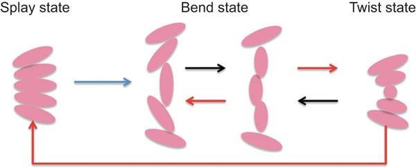
Transition of LC molecular states in a pi-cell.63 LC, liquid crystal.
The alignment conditions are challenging for LCOS device fabrication using rubbed alignment because the relatively high-tilt polyimide alignment layer requires a high curing temperature that degrades the reflectivity of the aluminum pixel surface.

SSFLCs
The surface-stabilized electro-optic effect in chiral smectic C LC64 can be used for phase-only LCOS devices primarily because of its ultrafast response speed and polarization independence.65 However, SSFLC can only provide binary phase-only light modulation. Although the subframe sequential technique is used to achieve different voltage levels and multi-level modulation that are available in FLC-LCOS holographic projection,37 this technique loses at least half of the incident light to symmetric diffraction orders. Moreover, it was observed that the maximum light efficiency (<50%) could be only achieved if the FLC switching angle was 90°. This angle requires highly specialized materials that tend to slow the response time such that the devices are comparable to the responses times of the nematic phase-only LCOS devices operating in the ECB electro-optic effect. In addition, large quantization noise occurs in SSFLC.33
The present study is restricted to analog (i.e., non-binary) phase-only devices because binary holograms have insufficient degrees of freedom for certain phase-only LCOS applications such as optical switching in telecommunication systems and high-quality image projection.
Summary
LC materials as a high-performance non-linear electro-optic medium are ideal for CMOS-based spatial light modulation devices because these materials not only have one of the largest known electro-optic coefficients but are also able to be driven directly by relatively low voltages. When an external electric field is applied, LC molecules re-orientate. Because of their optical birefringence, the effective optical refraction coefficient changes accordingly, resulting in a modulation in the phase retardation as controlled by the applied voltage. Therefore, for an effective phase modulation, phase-only LCOS devices benefit from an ECB electro-optic effect with a zero-twisted configuration, a small pre-tilt angle and an anti-parallel alignment.
OCB (pi-cell) might be a candidate for phase-only LCOS devices in the future due to its faster response; however, currently, there are several issues, such as the high pre-tilt angle requirement, unwanted twist state during switching and high-temperature surface treatment. Furthermore, in a pi-cell, the voltage for overcoming the threshold must be much larger than the critical voltage such that the LC can be deformed from the splay state to the bend state, which necessitates a much higher effective threshold in a pi-cell than in an anti-parallel alignment rubbed device. This requirement is a problem when using smaller pixels and the relatively low maximum voltages that are available from current silicon backplanes. However, for pi-cells, the voltage can be reduced by increasing the dielectric anisotropy or using a low anchoring energy or high pre-tilt alignment.66 Therefore, pi-cells are still being investigated as an alternative electro-optic effect, which might be used in phase-only LCOS devices.
The TN structure is not suitable for phase-only LCOS devices because both the phase and polarization need to be modulated, which will cause difficulty in phase-only holography. The VAN is not considered as a candidate either because the small value of the negative dielectric anisotropy of the required materials leads to a higher threshold voltage. FLC-LCOS can only provide binary switching (0/1), which results in a lower light efficiency and high quantization noise in the replay field of holograms. Binary holograms using SSFLC have inadequate degrees of freedom for phase-only LCOS devices.
Considering the application of the ECB electro-optic effect for phase-only LCOS devices, the nematic LC materials must have a higher birefringence (i.e., the required thickness for the device can be smaller) and consequently a faster response speed. In addition, the materials must have a reasonably high positive dielectric anisotropy such that they respond to low voltages. However, these materials have relatively high viscosities. This characteristic is common for highly anisotropic materials, which have a slow material response. Because the viscosity is a very temperature-dependent parameter, a solution might be to introduce an offset to some extent by raising the temperature. However, attempts to use higher birefringence mixtures resulted in instabilities at higher temperatures (50°C) or photochemical degradation when exposed to blue light.67
Requirements for the device and response time
Because an LCOS device can be either transmissive or reflective, the thickness of the LCOS device should be considered individually. For a reflective phase-only LCOS device with ECB electro-optic effect for 2π phase modulation and by ignoring the small pre-tilt angle, the LC layer is switched from planar to homeotropic. The phase retardation of light as it passes through an LCOS device is given by

where d is the thickness of the device (LC layer), Δn is birefringence and λ is the wavelength of incident light. Because current phase-only LCOS devices operate in a reflective mode, the total phase retardation is given by

If the phase modulation of phase-only LCOS devices is required to be 2π, the thickness is required to be

For other types of LCOS devices, for instance, the thickness of a reflective amplitude LCOS device should be reduced by half for π phase modulation, and the thickness of a transmissive amplitude LCOS device should be the same as a reflective phase-only LCOS device. Figure 9a illustrates that the thickness of the conventional and transmissive amplitude LCOS device should be at least ‘π’; Figure 9b illustrates that the thickness of the reflective amplitude LCOS device should be at least ‘π/2’; and Figure 9c demonstrates that the thickness of the reflective phase-only LCOS device should be at least ‘π’ to achieve 2π phase modulation.

Thickness comparison of the cross-sections of different types of LCOS devices (H=π). LCOS, liquid crystal on silicon.
Comparing a reflective amplitude modulation LCOS device with π phase retardation, the thickness of a reflective phase-only device must be doubled for 2π phase retardation. Therefore, the switching speed for phase-only LCOS is approximately four times slower than amplitude-modulated LCOS devices. The rise and decay times depend on the square of the device thickness (d2), which dominates the response time. The thickness of LCOS devices can only be minimized by increasing the birefringence. For the infrared device, the thickness is especially large, which exaggerates the effect of the flow; thus, the response time might be observed to be significantly slower than expected.
Silicon backplane and addressing scheme
The functionalities of silicon backplane LCOS devices have been improved by the development of CMOS processes. Compared with a conventional CMOS manufacturing process, the LCOS backplane require two special processes:68 first, the top metal layer must have a high reflectivity to reflect the incident light sufficiently; second, manufacturers must retain an earlier process with a larger feature size than the current state-of-the-art. This requirement is necessary to ensure that there is sufficient voltage from a standard CMOS process, which must be available at each pixel to switch the LC rapidly. The LCOS silicon backplanes currently available use CMOS in the range of 0.18–0.35 µm. Example processes include Fujitsu (0.18 µm), Chartered (0.18 µm) and Citizen (0.25 µm). All of these processes use logic supplies of less than 3.3 V and are available with 5- or 12-V (higher) processes for driving the pixels. In a reflection mode phase-only LCOS device, the CMOS silicon backplane performs several functions:
The pixel array consists of an array of aluminum mirrors with pixel circuitry containing signal lines, gate lines and transistors buried beneath the pixels to obtain the maximum fill factor22 (>90%).
The density and complexity possible with CMOS circuitry allows for the integration of row and column access circuitry onto the LCOS chip and the use of much more sophisticated pixel circuitry than is possible with thin film transistor active matrix displays.
Rapid row-by-row scanning over the entire pixel array is used to display each subframe of information. Each pixel is set up with an appropriate drive voltage such that the LC layer responds to the RMS (root mean square) of the applied voltage.
Two types of pixel addressing circuits can be distinguished: dynamic random-access memory (DRAM)69-based and static random-access memory (SRAM)69-based circuitries.
DRAM-based pixel circuitry
The advantages of DRAM pixel design are the small footprint, simplicity and unipolarity of the circuit. Therefore, the maximized density and performance of the circuit are allowed with no additional complementary structures. The disadvantages of such a design are the low driving voltage in use and the short retention time of data voltage levels due to charge leakage, which leads to the reduction of the switching speed and also an incomplete switching process of LC materials. Thus, refreshing in the pixel array is required due to the voltage discharge and may cause the phase flickers70 during the duration of a phase-modulation process. The pixel-level charge leakage problem here cannot be resolved by adding a storage capacitor as in the standard liquid crystal display pixel circuitry due to the very limited pixel footprint area in the LCOS case.
SRAM-based pixel circuitry
The SRAM pixel design is able to provide stable and full voltage to the backplane, and therefore, the LC materials are able to be fully switched with a maximized speed. However, to connect the pixel array, additional complimentary nodes are required for the SRAM pixel design. Thus, a larger footprint than that of a DRAM design is needed. Furthermore, extra complimentary nodes are subject to insufficient protection for latch-up in a pixel, which can be induced in the substrate by the presence of light.
To meet the stringent requirement of voltage level stability for the minimum phase flickers of phase-only LCOS chips, SRAM-based pixel circuitry has been used in almost all of the designs. As the pixel size itself is becoming increasingly smaller from 15 µm a few years ago to 3–4 µm currently, designing an SRAM cell with the smallest footprint remains a challenge.
There are two typical addressing schemes for LCOS devices: the so-called ‘analog driving scheme’ and ‘digital driving scheme’ (pulse width modulation). The analog driving scheme is inherently based on the DRAM pixel circuitry that allows an analog voltage to be stored on a pixel capacitor during each subframe period, and the voltage across the LC is appropriately conserved until it is refreshed. This scheme allows the desired voltage to be refreshed at each subframe scan.
Digital driving schemes, however, are based on SRAM pixel circuitry that allows digital pulses to be applied for different periods.71,72,73 These pulses are binary in nature and are applied to the LC. In this case, different average voltage levels are implemented using pulse width modulation on the basis that LCs respond to the RMS value of the applied voltage waveform.
If fast LCs, electro-optic effects are used to achieve high frame rates, and the LC may deviate from a time-averaged RMS response and may start responding to individual pulses within the frame period. This reaction is of no consequence in a conventional projector because the eye will perceive the RMS response of the fluctuating intensity; however, this phenomenon seriously degrades the replay of holograms, which are unable to time average the temporal fluctuations. The result is spatial noise in the replayed image. Thus, analog DRAM silicon backplanes are preferred for holographic applications. Hence, a DRAM (analog) is selected for the phase-only LCOS device.
Some research institutions and companies that have developed nematic LCOSs for phase-only modulation, such as ‘Holoeye’, also offer research-oriented devices, such as LC-R 2500, a 45° twisted nematic based on a Philips 1024×768 pixel backplane with a custom interface, high contrast and good gap tolerance,74 an ‘LETO’ reflective LCOS with high definition resolution, pixel pitch 6.4 µm, 0.55″ diagonal and 75% reflectivity.75 ‘Holoeye’ supplies nematic LCOS devices modified for phase-only operation. The backplane used was from Aurora Systems Inc. (San Jose, CA, USA)76 and currently from Jasper Display Corp (Hsinchu, Taiwan, China).77 and achieves grey scale digitally using pulse width modulation to achieve multiple phase modulations.
Table 1 lists the major LCOS companies offering silicon backplane designs and some projector suppliers using LCOS technology including JVC and Forth Dimension Displays (Forth DD). The pitch indicates the inter-pixel spacing in microns, the fill factor relates to the percentage of pixel that forms a reflective mirror, the refresh rate expresses the driving scheme speed and the “array” means the pixelated area, expressed either as the length of the diagonal or as the width×height.
Algorithms of hologram generation for phase-only LCOS devices in real-time holography
One method of computing the phase pattern of a computer-generated hologram uses an iterative Fourier transform algorithm and is a degenerate problem requiring an optimisation process. Holograms use diffraction to route the light to the bright areas of the reconstructed image. The complex relationship between the hologram (or kinoform)79 and the reconstructed image is such that the image quality cannot be determined directly from the characteristics of the phase-modulating device as in the case for conventional displays. The hologram of the image is loaded on the phase-only LCOS device and illuminated by a collimated beam coming from a laser source. The image is reconstructed using the diffracted beam from the hologram, which is transformed by a Fourier transform lens, thereby forming an image at the far field.
In the past, static hologram patterns have been calculated using iterative algorithms in which pixels are changed one at a time. Boltzmann annealing algorithms80,81,82 (simulated annealing or direct binary search) are considered ideal for generating holograms. These algorithms are sometimes referred to as ‘pixel-flipping’ algorithms. An image can be recreated when a coherent light beam illuminates the hologram through the glass etched to form a phase hologram. The reconstructed image can be of very good quality using this method. However, due to the laborious nature of the algorithm, the calculation takes a long time to complete. Therefore, it is not currently suitable for real-time holographic projection. Gerchberg-Saxton83 suggested an iterative phase-retrieval algorithm that can calculate a phase-only diffraction pattern (or hologram) that can be replayed to produce a given intensity pattern. This class of algorithms does not involve ‘pixel-flipping’. These algorithms are sometimes called ‘Ping-Pong algorithms’. Fienup et al.84,85,86,87 improved this type of algorithm using ‘over-compensation’ methods to increase the calculation speed, which converge faster by providing feedback on the amplitude of the reconstruction of the image. Georgiou and Christmas88,89,90 improved the iterative algorithm called ‘Fienup with don’t care’ (‘Fidoc’) to facilitate real-time processing of the image; the algorithm is able to achieve significantly higher speed and excellent image quality by dispersing noise into a ‘don’t care’ area around the image. Therefore, this algorithm is compatible with phase-only LCOS devices for projection applications.
The LCOS technique was originally used in the display industries. Recently, it has begun to be used in areas such telecommunication, medical sciences (e.g., ophthalmology91), national defense industry92 and atmospheric sciences for the correction of atmospheric turbulence.93,94 There are two classes of phase-only applications: first, where the polarization of the light is known and fixed, e.g., in projectors, and second, in telecommunication systems, where the polarization can vary. These two classes of application can exploit different electro-optic structures.
In a holographic projection projector,89 a single pixel of the reconstructed image is formed by all the hologram pixels, and a single hologram pixel contributes to all the image pixels of the reconstructed image. The development of high-power, compact light sources and fast Fourier transform processors make the holographic projection technology a practical proposition. Alps Electric UK and Light Blue Optics95 are two companies currently developing holographic projectors, automotive head-up displays, interactive projectors, etc.
Optical beam deflection in the telecommunication networks is one of the major applications of phase-only LCOS devices. In fiber optic telecommunication networks, the data are usually encoded on light beams with wavelengths in the C-Band at approximately 1.5 μm in the near infrared. This encoding necessitates special LCOS devices with a thickness selected to yield a phase excursion of 2π at these wavelengths. There are many related references to optical switching based on LCOS technology. For instance, Jeon and Sawchuk96 presented a switch using a variable fixed periodic grating for an optical interconnections system, which is neither a computer generated hologram nor a dynamic one. However, this work provided the good idea that the LC spatial light modulator might be applicable to beam deflection. Barnes et al.97 reported the use of a phase grating on a transmission LC panel. However, this device was not optimized for phase-only operation. Collings et al.98 demonstrated that a grating could be displayed on an optically addressed SLM (FLC-OASLM) by interfering two light beams, which yields a more complicated optical system than the standard approach of using a phase-only LCOS device directly. In 1991, O’Callaghan65 demonstrated polarization-independent phase-only binary gratings. This technique was used in the UK ROSES optical switches project.36 However, as mentioned for an FLC-LCOS system, the loss is too high and is doubled when the fibers are optically coupled at both the input and output ports of a switch.99 Nematic LC devices avoid most of these diffraction efficiency losses. However, because the nematic electro-optic effects are polarization sensitive and make the devices polarization independent, a quarter wave plate100 must be applied on the reflective mirror. The normal thickness of a quarter wave plate is approximately 3 µm, which is thicker than the LC layer. Thus, the available voltage at the pixels is significantly lowered, thereby decreasing the LC response time. Crossland et al.101 demonstrated an improvement in diffraction efficiency (>77%) using nematic LCs. polarization independence can also be achieved by splitting the optical signal beam into its two separate orthogonal polarization components and switching these independently. This process doubles the complexity of the optics but avoids the quarter waveplate. Phase-only nematic LCOS devices are now becoming the dominant optical switch technology in reconfigurable add-drop multiplexers (ROADMs).102, 103,104,105 One of the best performances for ROADMs was demonstrated by Robertson et al.19 recently and implements a multifunctional 1×9 wavelength selective switch (WSS) based on a phase-only nematic LCOS device with −7.6 dB of insertion loss and −19.4 dB of the worst-case crosstalk for a channel spacing of 100 and 200 GHz. These devices offer better control of the optical wavefronts and more flexibility than MEMS (micro electro mechanical systems) devices.
Optical tweezers based on LCOS technology that tether tiny particles to optical traps have become a fruitful application for the study of nanoparticles. This technique is increasingly useful for controlling and probing matter at length scales from nanometers to millimeters. Originally, Ashkin106 reported the first observation of the acceleration of freely suspended particles by the forces of radiation pressure from continuous visible wavelength laser light. Later, he published107 the observation of a single-beam gradient-force optical trap for dielectric particles in air. In 2002, Curtis reported methods for creating larger numbers of high-quality optical traps in arbitrary three-dimensional (3D) configurations that are dynamically reconfigured by computer control. These systems use real-time holograms on phase-only LCOS devices to generate the optical traps. By employing a ferroelectric LC spatial light modulator, a fast switching speed is obtained. Heggarty et al.108 published a very rapid reconfiguration of trap geometries, high-speed particle movement and tweezer arrays using FLC-LCOS. The basis of performance improvement for optical tweezers consists of trap intensity control, spatial variations of the phase response or eliminating the amount of light away from the traps.
Conclusions
Real-time holography using phase-only holograms (dynamic kinoforms) displayed by LCOS devices is now emerging as a useful technology. Applications include head-up displays, telecommunication devices (WSSs and ROADMs) and future holographic 3D displays. Many of the new applications are under development, and suitable LCOS devices are not yet widely available. In other words, the device technology itself remains at its early stage of maturity and is currently based on modified versions of amplitude-modulating LCOS devices (originally made for rear-projection TVs). Significant changes need to be made in these devices to allow them to be used in holographic applications, where the optical quality required is more stringent. This paper debates aspects of the engineering of nematic phase-only LCOS devices for applications of real-time holography. This application will enable progress to be made with the cutting-edge application research and will also allow the development of better devices (e.g., by improving the LC materials and electro-optic effect). The availability of high-yield CMOS backplanes and efficient methods of device testing and progression of new device concepts are essential if the subject is to mature rapidly for the fast deployment of the phase-only LCOS technology.
References
Vettese D . Microdisplays: liquid crystal on silicon. Nat Photonics 2010; 4: 752–754.
Zhang ZC, Jeziorska-Chapman AM, Collings N, Pivnenko M, Moore J et al. High quality assembly of phase-only liquid crystal on silicon (LCOS) devices. J Display Technol 2011; 7: 120–126.
Choubey A, Andros F, Sammakia BG . Study of assembly processes for liquid crystal on silicon (LCoS) microdisplays. IEEE Trans Compon Packag Technol 2005; 28: 303–310.
Kazlas PT, Johnson KM, McKnight DJ . Miniature liquid-crystal-on-silicon display assembly. Opt Lett 1998; 23: 972–974.
Ju TH, Lin W, Lee YC, Mcknight DJ, Johnson KM . Packaging of a 128 by 128 liquid-crystal-on-silicon spatial light modulator using self-pulling soldering. IEEE Photonics Technol Lett 1995; 7: 1010–1012.
Collings N, Davey T, Christmas J, Chu DP, Crossland B . The applications and technology of phase-only liquid crystal on silicon devices. J Display Technol 2011; 7: 112–119.
Wilkinson TD, Henderson CD, Leyva DG, Crossland WA . Phase modulation with the next generation of liquid crystal over silicon technology. J Mater Chem 2006; 16: 3359–3365.
Zhang ZC, Yang HN, Robertson B, Redmond M, Pivnenko M et al. Diffraction based phase compensation method for phase-only liquid crystal on silicon devices in operation. Appl Optics 2012; 51: 3837–3846.
Engström D, Persson M, Bengtsson J, Goksör M . Calibration of spatial light modulators suffering from spatially varying phase response. Opt Express 2013; 21: 16086–16103.
Reichelt S . Spatially resolved phase-response calibration of liquid-crystal-based spatial light modulators. Appl Opt 2013; 52: 2610–2618.
Cibula MA, McIntyre DH . General algorithm to optimize the diffraction efficiency of a phase-type spatial light modulator. Opt Lett 2013; 38: 2767–2769.
Yang H, Robertson B, Yu D, Zhang Z, Chu DP . Origin of transient crosstalk and its reduction in phase-only LCOS wavelength selective switches. J Lightwave Technol 2013; 31: 3822–3829.
Dai HT, Xu KS, Liu YJ, Wang X, Liu JH . Characteristics of LCoS phase-only spatial light modulator and its applications. Opt Commun 2004; 238: 269–276.
Hussain A, Martínez JL, Campos J . Holographic superresolution using spatial light modulator. J Eur Opt Soc Rapid Publ 2013; 8: doi: 10.2971/jeos.2013.13007.
Hussain A, Martínez JL, Lizana A, Campos J . Super resolution imaging achieved by using on-axis interferometry based on a Spatial Light Modulator. Opt Express 2013; 21: 9615–9623.
Guo CS, Rong ZY, Wang SZ . Double-channel vector spatial light modulator for generation of arbitrary complex vector beams. Opt Lett 2014; 39: 386–389.
Reichelt S, Häussler R, Fütterer G, Leister N, Kato H et al. Full-range, complex spatial light modulator for real-time holography. Opt Lett 2012; 37: 1955–1957.
Zeng X, Bai J, Hou CL, Yang GG . Compact optical correlator based on one phase-only spatial light modulator. Opt Lett 2011; 36: 1383–1385.
Robertson B, Yang HN, Redmond MM, Collings N, Moore JR et al. Demonstration of multi-casting in a 1×9 LCOS wavelength selective switch. J Lightwave Technol 2014; 32: 402–410.
Chou HH, Zhang F, Wilkinson TD, Collings N, Crossland WA . Implementation of a 6×6 free-space optical fiber ribbon switch for storage area networks. J Lightwave Technol 2012; 30: 1719–1725.
Robertson B, Zhang ZC, Yang HN, Redmond MM, Collings N et al. Application of the fractional Fourier transform to the design of LCOS based optical interconnects and fiber switches. Appl Opt 2012; 51: 2212–2222.
Robertson B, Zhang ZC, Redmond MM, Collings N, Liu JS et al. Use of wavefront encoding in optical interconnects and fiber switches for cross talk mitigation. Appl Opt 2012; 51: 659–668.
Martínez JL, Martínez-García A, Moreno I . Wavelength-compensated color Fourier diffractive optical elements using a ferroelectric liquid crystal on silicon display and a color-filter wheel. Appl Opt 2009; 48: 911–918.
Zheng M, Ogura Y, Tanida J . Three-dimensional dynamic optical manipulation by combining a diffractive optical element and a spatial light modulator. Opt Rev 2008; 15: 105–109.
Lizana A, Moreno I, Márquez A, Iemmi C, Fernández E et al. Time fluctuations of the phase modulation in a liquid crystal on silicon display: characterization and effects in diffractive optics. Opt Express 2008; 16: 16711–16722.
Ernstoff M, Leupp A, Little M, Peterson H . Liquid crystal pictorial display. In: Proceedings of the 1973 International Electron Devices Meeting; 3-5 December 1973; Washington, DC, USA. IEEE: New York, USA, 1973: pp 548–551.
Crossland WA, Ayliffe PJ, Ross PW . A dyed-phase-change liquid-crystal display over a MOSFET switching array. Proc SID 1982; 23: 15–22.
Collings N, Crossland WA, Ayliffe PJ, Vass DG, Underwood I . Evolutionary development of advanced liquid crystal spatial light modulators. Appl Opt 1989; 28: 4740–4747.
Underwood I, Vass DG, Sillitto RM, Bradford G, Fancey NE et al. High-performance spatial light modulator. Proc SPIE 1991; 1562: 107–115; doi: 10.1117/12.50776.
Washwell ER, Gebelein RJ, Gheen GO, Armitage D, Handschy MA . Miniature hybrid optical correlators: device and system issues. Proc SPIE 1990; 1297: 64–71; doi: 10.1117/12.21298.
Juday RD . Correlation with a spatial light modulator having phase and amplitude cross coupling. Appl Opt 1989; 28: 4865–4869.
Sharp JH, MacKay NE, Tang PC, Watson IA, Scott BF et al. Experimental systems implementation of a hybrid optical–digital correlator. Appl Opt 1999; 38: 6116–6128.
Dasgupta P, Das MK, Das B . Physical properties of three liquid crystals with negative dielectric anisotropy from X-ray diffraction and optical birefringence measurements. Mol Cryst Liq Cryst 2011; 540: 154–161.
Kohns P, Schirmer J, Muravski AA, Yakovenko SY, Bezborodov V et al. Birefringence measurements of liquid crystals and an application: an achromatic waveplate. Liq Cryst 1996; 21: 841–846.
Wu ST, Efron U, Hess LD . Birefringence measurements of liquid crystals. Appl Opt 1984; 23: 3911–3915.
Crossland WA, Manolis IG, Redmond MM, Tan KL, Wilkinson TD et al. Holographic optical switching: the “ROSES” demonstrator. J Lightwave Technol 2000; 18: 1845–1854.
Buckley E . Holographic laser projection. J Display Technol 2011; 7: 135–140.
Stamm S, Riethoven JJ, Le Texier V, Gopalakrishnan C, Kumanduri V et al. ASD: a bioinformatics resource on alternative splicing. Nucleic Acids Res 2006; 34( suppl 1): D46–D55.
McKnight DJ, Vass DG, Sillitto RM . Development of a spatial light modulator: a randomly addressed liquid-crystal-over-nMOS array. Appl Opt 1989; 28: 4757–4762.
Soref RA, Rafuse MJ . Electrically controlled birefringence of thin nematic films. J Appl Phys 1972; 43: 2029–2037.
Labrunie G, Robert J . Transient behavior of the electrically controlled birefringence in a nematic liquid crystal. J Appl Phys 1973; 44: 4869–4874.
Armitage D, Kinell DK . Miniature spatial light modulators. Proc SPIE 1990; 1296: 158–165.
Cotter LK, Drabik TJ, Dillon RJ, Handschy MA . Ferroelectric-liquid-crystal/silicon-integrated-circuit spatial light modulator. Opt Lett 1990; 15: 291–293.
Armitage D, Kinell DK . Liquid-crystal integrated silicon spatial light modulator. Appl Opt 1992; 31: 3945–3949.
McKnight DJ, Johnson KM, Serati RA . 256×256 liquid-crystal-on-silicon spatial light modulator. Appl Opt 1994; 33: 2775–2784.
Schadt M, Helfrich W . Voltage-dependent optical activity of a twisted nematic liquid crystal. Appl Phys Lett 1971; 18: 127–128.
Fergason JL . Display devices utilizing liquid crystal light modulation. US Patent US3731986; 1973.
Gibbons WM, Shannon PJ, Sun ST, Swetlin BJ . Surface-mediated alignment of nematic liquid crystals with polarized laser light. Nature 1991; 351: 49–50.
Creagh LT, Kmetz AR . Mechanism of surface alignment in nematic liquid crystals. Mol Cryst Liq Cryst 1973; 24: 59–68.
Khoo IC, Wu ST . Optics and Nonlinear Optics of Liquid Crystals. Singapore: World Scientific, 1993.
Wu ST, Yang DK . Fundamentals of Liquid Crystal Devices. New York: John Wiley & Sons, 2006.
Raynes EP . Optically active additives in twisted nematic devices. Rev Phys Appl 1975; 10: 117–120.
Hiji N, Kyozuka S, Yamamoto S . Reflective liquid crystal display. US Patent US5953089; 1999.
Chigrinov VG . Liquid Crystal Devices: Physics and Applications. Norwood, MA: Artech House, 1999.
Crossland WA, Wilkinson TD, Manolis IG, Redmond MM, Davey AB . Telecommunications applications of LCOS devices. Mol Cryst Liq Cryst 2002; 375: 1–13.
Kelly J . Application of liquid crystal technology to telecommunication devices. In: Optical Fiber Communication Conference and Exposition and the National Fiber Optic Engineers Conference, OSA Technical Digest Series (CD), 2007: paper NThE1.
Bos PJ, Koehler/beran KR . The pi-cell: a fast liquid-crystal optical-switching device. Mol Cryst Liq Cryst 1984; 113: 329–339.
Takatoh K, Sakamoto M, Hasegawa R, Koden M, Itoh N et al. Alignment Technology and Applications of Liquid Crystal Devices. London: CRC Press, 2005.
Deuling HJ . Deformation of nematic liquid crystals in an electric field. Mol Cryst Liq Cryst 1972; 19: 123–131.
Acosta EJ, Towler MJ, Walton HG . The role of surface tilt in the operation of pi-cell liquid crystal devices. Liquid Cryst 2000; 27: 977–984.
Nakamura H, Noguchi M . Bend transition in pi-cell. Jpn J Appl Phys 2000; 39: 6368–6375.
Lee SH, Kim TJ, Lee GD, Yoon TH, Kim JC . Geometric structure for the uniform splay-to-bend transition in a π-cell. Jpn J Appl Phys 2003; 42: L1148–L1151.
Inoue I, Miyashita T, Uchida T, Yamada Y, Ishii Y . A new solution for splay-to-bend transition in OCB mode with a twisted area. J Soc Inf Display 2003; 11: 571–576.
Clark NA, Lagerwall ST . Submicrosecond bistable electro-optic switching in liquid crystals. Appl Phys Lett 1980; 36: 899–901.
O’Callaghan MJ, Handschy MA . Diffractive ferroelectric liquid-crystal shutters for unpolarized light. Opt Lett 1991; 16: 770–772.
Wu WC, Chen YF, Chen SF, Chen HMP . Critical voltage reduction by alignment layer modification in pi-cells. In: Proceedings of the 7th International Display Manufacturing Conference; 3–6 July 2007; Taiwan, China. Society for Information Display: Los Angeles, CA, USA, 2007.
Aad G, Abbott B, Abdallah J, Abdelalim AA, Abdesselam A et al. Measurement of the inclusive isolated prompt photon cross section in pp collisions at
 with the ATLAS detector. Phys Rev D 2011; 83: 052005.
Moore JR, Collings N, Crossland WA, Davey AB, Evans M et al. The silicon backplane design for an LCOS polarization-insensitive phase hologram SLM. IEEE Photonics Technol Lett 2008; 20: 60–62.
Prince B . Semiconductor Memories: A Handbook of Design, Manufacture and Application. 2nd Ed. New York: John Wiley & Sons, 1996.
García-Márquez J, López V, González-Vega A, Noé E . Flicker minimization in an LCoS spatial light modulator. Opt Express 2012; 20: 8431–8441.
Collings N, Crossland WA, Ayliffe PJ, Vass DG, Underwood I . Evolutionary development of advanced liquid crystal spatial light modulators. Appl Opt 1989; 28: 4740–4747.
Lueder E . Liquid Crystal Displays: Addressing Schemes and Electro-optical Effects. New York: John Wiley & Sons, 2010.
Kang JS, Kwon OK . Digital driving method for low frame frequency and 256 gray scales in liquid crystal on silicon panels. J Display Technol 2012; 8: 723–729.
Lu M . Nematic liquid-crystal technology for Si wafer-based reflective spatial light modulators. J Soc Inf Display 2002; 10: 37–47.
Osten W, Reingand N . Optical Imaging and Metrology: Advanced Technologies. New York: John Wiley & Sons, 2012.
Jepsen ML, Ammer MJ, Bolotski M, Drolet JJ, Gupta A et al. High resolution LCOS microdisplay for single-, double-or triple-panel projection systems. Displays 2002; 23: 109–114.
Hudson EL . Multi-mode pulse width modulated displays. US Patent US7852307; 2010.
Crossland WA, Vass D, Collings N . Spatial light modulators. US Patent US5339090; 1994.
Gallagher NC, Liu B . Method for computing kinoforms that reduces image reconstruction error. Appl Opt 1973; 12: 2328–2335.
Kirkpatrick S . Optimization by simulated annealing: quantitative studies. J Stat Phys 1984; 34: 975–986.
Seldowitz MA, Allebach JP, Sweeney DW . Synthesis of digital holograms by direct binary search. Appl Opt 1987; 26: 2788–2798.
Kirk AG, Hall TJ . Design of binary computer generated holograms by simulated annealing: coding density and reconstruction error. Opt Commun 1992; 94: 491–496.
Gerchberg RW, Saxton WO . A practical algorithm for the determination of the phase from image and diffraction plane pictures. Optik 1972; 35: 237–246.
Fienup JR . Reconstruction of an object from the modulus of its Fourier transform. Opt Lett 1978; 3: 27–29.
Fienup JR . Iterative method applied to image reconstruction and to computer-generated holograms. Opt Eng 1980; 19: 297–305.
Fienup JR . Phase retrieval algorithms: a comparison. Appl Opt 1982; 21: 2758–2769.
Fienup JR, Wackerman CC . Phase-retrieval stagnation problems and solutions. JOSA A 1986; 3: 1897–1907.
Georgiou A, Christmas J, Collings N, Moore J, Crossland WA . Aspects of hologram calculation for video frames. J Opt A: Pure Appl Opt 2008; 10: 035302.
Georgiou A, Christmas J, Moore J, Jeziorska-Chapman A, Davey A et al. Liquid crystal over silicon device characteristics for holographic projection of high-definition television images. Appl Opt 2008; 47: 4793–4803.
Matusik W, Pfister H . 3D TV: a scalable system for real-time acquisition, transmission, and autostereoscopic display of dynamic scenes. ACM Trans Graph 2004; 23: 814–824.
Manzanera S, Prieto PM, Ayala DB, Lindacher JM, Artal P . Liquid crystal adaptive optics visual simulator: application to testing and design of ophthalmic optical elements. Opt Express 2007; 15: 16177–16188.
Bagwell BE, Wick DV, Batchko R, Mansell JD, Martinez T et al. Liquid crystal based active optics. Proc SPIE 2006; 6289: 628908.
Mu Q, Cao Z, Hu L, Li D, Xuan L . Adaptive optics imaging system based on a high-resolution liquid crystal on silicon device. Opt Express 2006; 14: 8013–8018.
Cao Z, Mu Q, Hu L, Li D, Peng Z et al. Preliminary use of nematic liquid crystal adaptive optics with a 2.16-meter reflecting telescope. Opt Express 2009; 17: 2530–2537.
Routley PR, Corbett AD, Cable AJ, McCaughan GJ . Holographic image display systems. US Patent US0002019; 2011.
Jeon HI, Sawchuk AA . Optical crossbar interconnections using variable grating mode devices. Appl Opt 1987; 26: 261–269.
Barnes TH, Eiju T, Matsuda K, Ichikawa H, Taghizadeh MR et al. Reconfigurable free-space optical interconnections with a phase-only liquid-crystal spatial light modulator. Appl Opt 1992; 31: 5527–5535.
Collings N, Latham SG, Chittick RC, Crossland WA . Reconfigurable optical interconnect using an optically addressed light valve. Int J Opt Computing 1990; 1: 31–40.
Schwider J, Stork W, Streibl N, Völkel R . Possibilities and limitations of space-variant holographic optical elements for switching networks and general interconnects. Appl Opt 1992; 31: 7403–7410.
Stern TE, Bala K . Multiwavelength Optical Networks: A Layered Approach. Upper Saddle River: Prentice Hall PTR, 1999.
Crossland WA, Wilkinson TD, Manolis IG, Redmond MM, Davey AB . Telecommunications applications of LCOS devices. Mol Cryst Liq Cryst 2002; 375: 1–13.
Ahderom ST, Raisi M, Alameh KE, Eshraghian K . Reconfigurable microphotonic add/drop multiplexer architecture. In: Proceedings of 2004 IEEE International Conference on Field-Programmable Technology; 6–8 December 2004; Brisbane, Australia. IEEE: New York, USA, 2004: pp 203–207.
Baxter G, Frisken S, Abakoumov D, Zhou H, Clarke I et al. Highly programmable wavelength selective switch based on liquid crystal on silicon switching elements. In: Proceedings of the Optical Fiber Communication Conference; 5–10 March 2006, Anaheim, CA, USA. IEEE: New York, USA, 2006: doi: 10.1109/OFC.2006.215365.
Roelens MA, Frisken S, Bolger JA, Abakoumov D, Baxter G et al. Dispersion trimming in a reconfigurable wavelength selective switch. J Lightwave Technol 2008; 26: 73–78.
Levinson FH . System for scheduling transmission of indexed and requested database tiers on demand at varying repetition rates. US Patent US5404505; 1995.
Ashkin A . Acceleration and trapping of particles by radiation pressure. Phys Rev Lett 1970; 24: 156–159.
Ashkin A, Dziedzic JM, Bjorkholm JE, Chu S . Observation of a single-beam gradient force optical trap for dielectric particles. Opt Lett 1986; 11: 288–290.
Hossack WJ, Theofanidou E, Crain J, Heggarty K, Birch M . High-speed holographic optical tweezers using a ferroelectric liquid crystal microdisplay. Opt Express 2003; 11: 2053–2059.
 with the ATLAS detector. Phys Rev D 2011; 83: 052005.
Acknowledgements
This work was supported by the National Natural Science Foundation of China (61307077), Beijing Natural Science Foundation (4144076) and China Postdoctoral Science Foundation (2013M530613). This work was also supported by an EPSRC Platform Grant for LC Photonics (EP/F00897X/1).
Author information
Authors and Affiliations
Corresponding authors
Rights and permissions
This work is licensed under a Creative Commons Attribution-NonCommercial-ShareAlike 3.0 Unported License. The images or other third party material in this article are included in the article's Creative Commons license, unless indicated otherwise in the credit line; if the material is not included under the Creative Commons license, users will need to obtain permission from the license holder to reproduce the material. To view a copy of this license, visit http://creativecommons.org/licenses/by-nc-sa/3.0/
About this article

Cite this article
Zhang, Z., You, Z. & Chu, D. Fundamentals of phase-only liquid crystal on silicon (LCOS) devices. Light Sci Appl 3, e213 (2014). https://doi.org/10.1038/lsa.2014.94
Received:
Revised:
Accepted:
Published:
Issue Date:
DOI: https://doi.org/10.1038/lsa.2014.94
Keywords
This article is cited by
-
Metasurface-enabled polarization-independent LCoS spatial light modulator for 4K resolution and beyond
Light: Science & Applications (2023)
-
Spatial light modulation for femtosecond laser manufacturing: Current developments and challenges
Science China Technological Sciences (2023)
-
High resolution 2D beam steerer made from cascaded 1D liquid crystal phase gratings
Scientific Reports (2022)
-
A full degree-of-freedom spatiotemporal light modulator
Nature Photonics (2022)
-
Tunable liquid crystal grating based holographic 3D display system with wide viewing angle and large size
Light: Science & Applications (2022)
