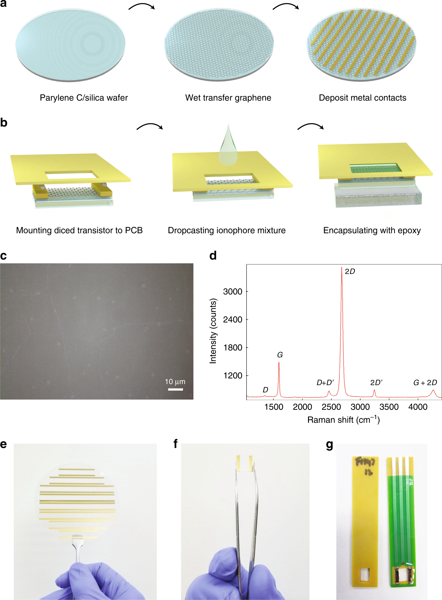
Fig. 1: Graphene ISFET Fabrication.
From: Selective ion sensing with high resolution large area graphene field effect transistor arrays

a Schematic of the fabrication process of the graphene ISFETs. 115 nm of parylene C was grown on a 100 mm diameter fused silica wafer. Graphene was grown via CVD on a 100 mm diameter Cu foil and wet-transferred to the target wafer using a PMMA handle. Ti/Au contacts were evaporated with the aid of a shadow mask. b The wafer was then diced into individual 1.1 cm × 1.1 cm devices, which were then mounted onto a PCB using silver epoxy. The ionophore mixture was dropcasted into the opening. Epoxy was used to encapsulate the back gate of the transistor. c Optical image with ×100 magnification of graphene monolayer transferred onto parylene C/fused silca wafer. Scale bar is 10 μm. d Raman spectra of 100 mm graphene wet-transferred onto target substrate. e An optical image showing a 4" graphene wafer on fused silica and parylene with gold contacts, ready to be diced into individual devices. f A single graphene device after being diced, and ready to be mounted on a PCB. fabrication process. g Top and bottom view of graphene ISFETs mounted on PCBs.
